3D metrology of CMP pads and grooves
Published on June 16, 2020
What are CMP pads and why measure them?
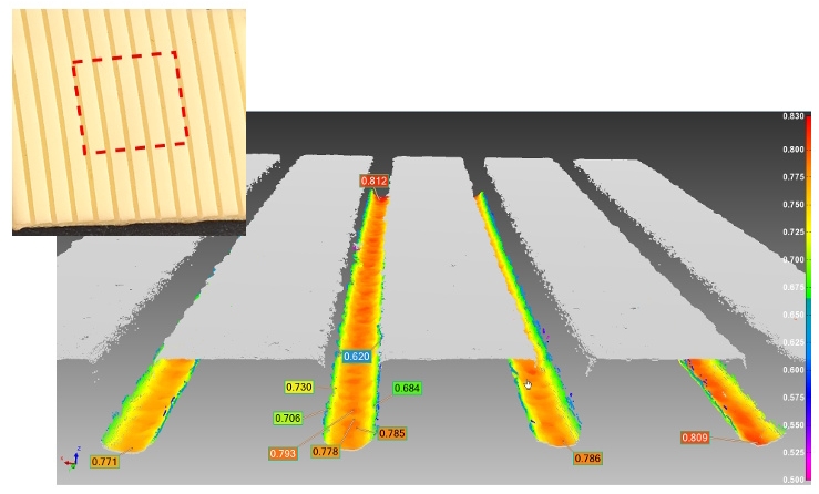
CMP pads are consumables used in the CMP (chemical mechanical polishing or planarization) process employed in the semi-conductor industry to flatten and polish silicon wafers. The pads are disk shaped, most commonly made from hard and porous polyurethane foam, and patterned with narrow high-aspect-ratio grooves (see image).
The function of the CMP process is to improve the performance of silicon wafers, which in turn are used in the development of high-performance microprocessor and memory chips. Since wafers are built up in several layers, each wafer typically undergoes the CMP process several times.
High-precision 3D metrology of CMP pads is required both in the pad manufacture and during the CMP process to ensure maximum process efficiency and efficacy.
How does the CMP process work?
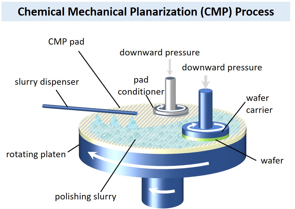
In the CMP process:
- The silicon wafer is mounted on a rotating wafer carrier and pressed against a CMP pad affixed on a rotating platen.
- At the same time, ultra-fine chemical polishing slurry is sprayed onto and channeled around the pad surface. Slurry distribution is done via tiny narrow grooves machined in specific patterns on the CMP pad surface.
- The corrosiveness of the slurry together with the asperities on the CMP pad surface wear away the wafer surface until the desired flatness and polish are achieved.
- To extend the lifespan of the CMP pad, the pad is typically reconditioned on a continuous or intermittent basis. This is done using a pad conditioner, which slices and pops open newly uncovered bubbles in the pad with diamond tips on its surface.
Why is quality control of CMP pads crucial?
First, both the silicon wafer and the CMP pads are costly items.
Second, the geometry and condition of CMP pad surfaces greatly affects CMP process efficacy.
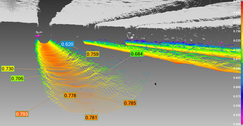
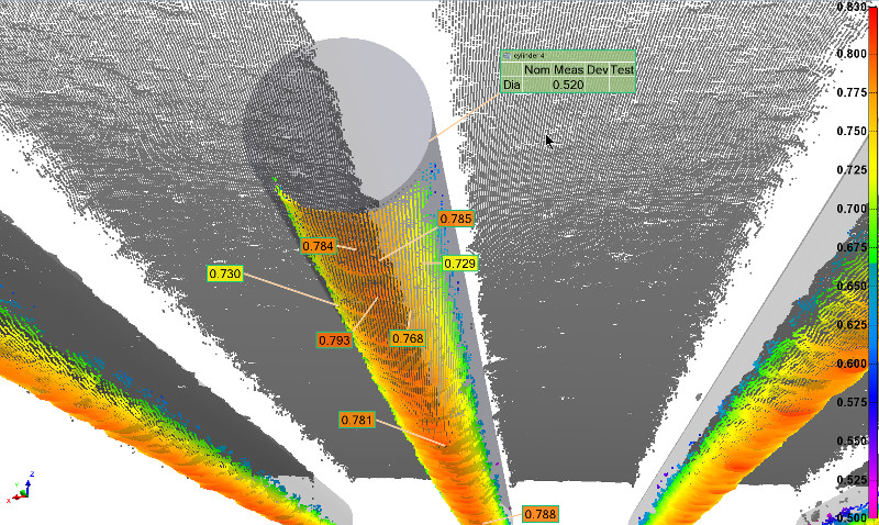
- For example, the grooves on CMP pads must be measured because the pattern, depth, and shape of these tiny channels influence slurry consumption and distribution, material removal rate (MRR), the rate of accumulation of polishing debris, as well as potential creation of scratches on wafers by this debris.
3D measurements for CMP pad manufacture and CMP process in general
Novacam 3D metrology systems are uniquely suitable to carry out fast, high-precision 3D metrology of:
- CMP pads, including the hard-to-measure grooves and lands (the surface between the grooves)
- CMP pad conditioners
- Wafers, including their flatness.
Novacam systems’ capabilities include:
- Non-contact 3D surface measurements with 1 μm (40 μin.) axial resolution
- Ability to scan high-aspect-ratio features such as the narrow CMP pad grooves
- High-speed surface acquisition – up to 100,000 3D measurements/sec
- Dimensional and roughness measurements with the same probe
- Ability to obtain long profiles
- Facility for automated measurement both in lab and in high-volume automated production.
Would you like to learn more?
- Check out our new CMP pad measurement application page
- Read Novacam’s “CMP Pad Metrology” application note [PDF, 4 pages].
Do you need to measure CMP pads, CMP pad conditioners and wafers?
Related links
Download application note “CMP Pad Metrology” [4 pages, PDF, 0.5 MB] for more details on this application
See related applications:


